


ESC concept:
Electrostatic chuck, also known as electrostatic chuck (English abbreviation: ESC or E-Chuck), is a fixture that uses the principle of electrostatic adsorption to clamp and fix the object to be adsorbed. It is suitable for vacuum and plasma environments, and its main function is to adsorb ultra-clean sheets (such as Silicon wafer), and keep the adsorbate in good flatness, which can suppress the deformation of the adsorbate in the process, and can also adjust the temperature of the adsorbate.
The structure and principle of ESC
1.Type: Basically divided into two categories. That is, the Coulomb class and the Jonsen-Rahbek (JR or Johnsen-Rahbek) class. Both types of suction cups rely on the same-sex attraction of electrostatic charges to fix the silicon wafer; the surface of the suction cup in contact with the wafer has a layer of dielectric. Ceramics are mostly used, the suction cups made of pure dielectric are Coulomb type, and the suction cups made of mixed dielectric are Jongsen thermal back type.

Coulomb force

Jonsen-Rahbek
2. Working principle
The practical application of ESC is divided into unipolar and bipolar (include bias voltage)

Unipolar

Bipolar embeds a DC electrode (smaller in size than a silicon wafer) in the dielectric layer of the chuck to connect to a high voltage (low current) DC power supply.
(1) The principle of suction
In the absence of plasma, when the DC electrode is connected to a high-voltage (low-current) DC power source, a polarized charge (for Coulomb chucks) develops on the surface of the dielectric. If it is a JR chuck, the dielectric surface not only has polarized charges, but also a large part of free charges, because the dielectric of the JR chuck has a certain conductivity. The surface charge of the dielectric will generate an electric field, which will further generate polarized charges on the surface of the wafer placed on the chuck (and possibly some free charges, depending on what kind of wafer and what kind of film is on the wafer surface, conductive or insulation).The charge distributed on the backside of the wafer is of opposite polarity to the charge distributed on the top of the chuck, so that the wafer is held by the chuck.
(2) The principle of release
a.Without plasma, if the high-voltage (low-current) DC power supply connected to the DC electrode(Embedded in the dielectric of the suction cup) is turned off, and if the charge distributed on the back of the wafer and the charge distributed on the chuck are both polarized charges, the wafer will be Released, that is, the suction automatically disappears.
b. Without plasma, if part of the charge distributed on the back of the chip and the charge distributed on the top of the sucker is free charge, even high-voltage (low-current) DC power supply connected to the DC electrode(Embedded in the dielectric of the suction cup) is turned off, the chip will not be fully released, namely because of residual charge and there are still certain electrostatic attraction. In this case, a reverse static voltage is usually required to force the removal of the residual charge before the chip can be released.
c.In the presence of plasma, due to self DC bias,even high-voltage (low-current) DC power supply connected to the DC electrode(Embedded in the dielectric of the suction cup) is turned off,when the chuck voltage is zero, the wafer will still be sucked by the chuck. This is because the DC self-bias acts as the chuck voltage. In some reaction chambers (not etching machines), the static voltage of a high-voltage (low-current) DC power supply is not even required, and the DC self-bias is sufficient for the task of holding the wafer. Therefore, after processing the wafer, a dechucking recipe is required to release the wafer, otherwise the wafer cannot be removed from the reaction chamber.
3. ESC Features
Generally speaking, the suction force of the JR type is larger than that of the Coulomb type. In the etching machine with high requirements on wafer temperature control, more and more Junsi hot back chucks are used, and the dielectric is usually a doped aluminum nitride ceramic material. Aluminum nitride has good thermal conductivity.
In the process of wafer processing, the reason why the wafer needs to be firmly sucked to the surface of the chuck is mainly to increase the heat transfer between the wafer and the chuck. In addition, the helium gas between the backside of the wafer and the surface of the chuck is an important medium for heat transfer.
In the suction cup, in addition to the DC electrodes, there are radio frequency electrodes. The RF electrodes are used to provide the RF bias power required during wafer processing. In some cases, the ESC is connected to the electrode through a filter.
In addition, circulation channels for coolant and air channels for helium are also required in the suction cup. Its design still requires special care and meticulousness. Moreover, its design is restricted by other aspects, such as the volume should not be too large, otherwise it will block or reduce the exhaust velocity of the reaction chamber.
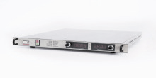
Wisman provides power supply for a full range of ESC, including:
High Voltage BiPolar Output (Positive/Negative),
Output polarity reversal function for easy wafer adsorption,
Ability to detect wafer condition by capacitive measurement (Coulomb chuck) or current measurement (JR chuck),
Analog and digital interfaces for easy integration into various systems,
High reliability, no mechanical relay design.
Wisman offers a wide range of design theory knowledge and manufacturing capabilities, so it can provide a wide range of custom products to meet a variety of requirements. Depending on the application, features include options such as high voltage bias/offset and RF filtering.


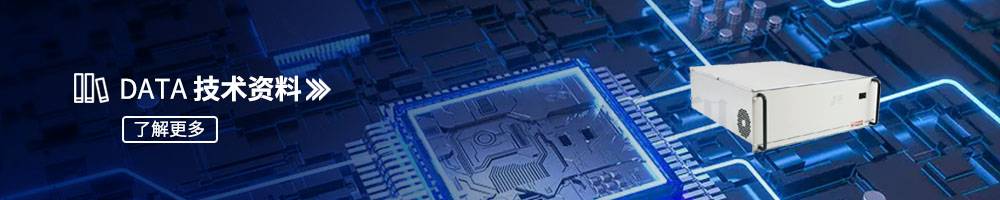
Applications in the field of semiconductors from Wisman high-voltage power supply
Today's complex semiconductor manufacturing processes require a variety of high-voltage power supply solutions, most of which have extremely demanding specifications. wisman's products run through the fabs from start to finish. From photolithography - power source - electrostatic wafer clamping - detection and testing equipment, our precise, low noise, high voltage power supply with high stability is the foundation that drives the rapid development of semiconductor technology.If you are working in wafer fabrication for the semiconductor industry, please contact wisman for more information. If standard products do not meet your needs, we can provide custom designs for OEM applications.